A detailed history of the processor
AMD Athlon (1999)
With the release of the Athlon processor in 1999, AMD’s status in the high performance realm was placed in concrete. The Athlon line continues to this day, with the highest clock speeds all operating off of various designs and improvements off of the Athlon series. But, the whole line started with the original Athlon classic. The original Athlon came at 500MHz. Designed at a 0.25 micron level, the chip boasted a super-pipelined, superscalar microarchitecture. It contained nine execution pipelines, a super-pipelined FPU and an again-enhanced 3dNow technology. These issues all rolled into one gave Athlon a real performance reputation. One notable feature of the Athlon is the new Slot interface. While Intel could play games by patenting Slot 1, AMD decided to call the bet by developing a Slot of their own – Slot A. Slot A looks just like Slot 1, although they are not electrically compatible. But, the closeness of the two interfaces allowed motherboard manufacturers to more easily manufacturer mainboard PCBs that could be interchangeable. They would not have to re-design an entire board to accommodate either Intel or AMD – they could do both without too much hassle.
Also notable with the release of Athlon was the entirely new system bus. AMD licensed the Alpha EV6 technology from Digital Equipment Corporation. This bus operated at 200MHz, faster than anything Intel was using. The bus had a bandwidth capability of 1.6 GB/s.
Athlon has gone through revisions and improvements and is still being used and marketed. In June of 2000, AMD released the Athlon Thunderbird. This chip came with an improved 0.18 micron design, on-die full speed L2 cache (new for Athlon), DDR RAM support, etc. It is a real workhorse of a chip and has a reputation for being able to be pushed well beyond the speed rating as assigned by AMD. Overclocker’s paradise. Thunderbird was also released in Socket A (or Socket 462) format, so AMD was now returning to its socketed roots just as Intel had already done by this time.
In May 2001, AMD released Athlon “Palomino”, also dubbed the Athlon 4. While the Athlon had now been out for about 2 years, it was now being beaten by Intel’s Pentium IV. The direct competition of the Pentium III was on its way to the museum already, and Athlon needed a boost to keep up with the new contender. The answer was the new Palomino core. The original intention of Palomino was to expand off of the Thunderbird chip, by reducing heat and power consumption. Due to delays, it was delayed and it ended up being beneficial. The chip was released first in notebook computers. AMD-based notebooks, until this time, were still using K6-2’s and K6-3’s and thus AMD’s reputation for performance in the mobile market was lacking. So, Athlon 4 brought AMD to the line again in the mobile market. Athlon 4 was later released to the desktop market, workstations, and multiprocessor servers (with its true dual processor support). Palomino made use of a data pre-fetch cache predictor and a translation look-aside buffer. It also made full use of Intel’s SSE instruction set. The chip made use of AMD’s PowerNow! technology, which had actually been around since the K6-2 and 3 days. It allows the chip to change its voltage requirements and clock speed depending on the usage requirement of the time. This was excellent for making the chip appropriate for power-sensitive apps such as mobile systems.
When AMD released the Palomino to the desktop market in October of 2001, they renamed the chip to Athlon XP, and also took on a slightly different naming jargon. Due to the way Palomino executes instructions, the chip can actually perform more work per clock cycle than the competition, namely Pentium IV. Therefore, the chips actually operate at a slower clock speed than AMD makes apparent in the model numbers. They chose to name the Athlon XP versions based on the speed rating of the processor as determined by AMD and their own benchmarking. So, for example, the Athlon XP 1600+ performs at 1.4 GHz, but the average computer user will think 1.6 GHz, which is what AMD wants. But, this is not to say that AMD is tricking anybody. In fact, these chips to perform like the Thunderbird at the rated speed, and perform quite well when stacked against the Pentium IV. In fact, the Athlon XP 1800+ can out-perform the Pentium IV at 2 GHz. Besides the naming, the XP was basically the same as the mobile Palomino released a few months earlier. It did boast a new packaging style that would help AMD’s release of 0.13 micron design chips later on. It also operated on the 133MHz front-side bus (266MHz when DDR taken into account). AMD continued to use the Palomino core until the release of the Athlon XP 2100+, which was the last Palomino.
In June of 2002, AMD announced the 0.13 micron Thoroughbred-based 2200+ processor. The move was more of a financial one, since there are no real performance gains between Palomino and Thoroughbred. Nonetheless, the smaller more means AMD can product more of them per silicon wafer, and that just makes sense. AMD is really taunting everyone with news of the coming ClawHammer core, which will be AMD’s next big move. But, with that chip still in the development and testing phase at this point, ClawHammer is not yet ready. Until it is, AMD will keep us mildly entertained with Thoroughbred and keep Intel sweating.
Celeron II (2000)
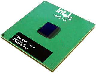
Just as the Pentium III was a Pentium II with SSE and a few added features, the Celeron II is simply a Celeron with a SSE, SSE2, and a few added features. The chip is available from 533 MHz to 1.1 GHz. This chip was basically an enhancement of the original Celeron, and it was released in response to AMD’s coming competition in the low-cost market with the Duron. The PSN of the Pentium III had been disabled in the Celeron II, with Intel stating that the feature was not necessary in the entry-level consumer market. Due to some inefficiencies in the L2 cache and still using the 66MHz bus (unless you overclock), this chip would not hold up too well against the Duron despite being based on the trusted Coppermine core. Celeron II would not be released with true 100 MHz bus support until the 800MHz edition, which was put out at the beginning of 2001.
Duron (2000)
In April of 2000, AMD released the Duron “Spitfire”. Spitfire came primarily out of the Athlon Thunderbird lineage, but it had a lighter load of cache onboard, ensuring that it was not a contender in the performance realm with its big cousin. The chip had a 128 KB L1 cache, but only 64 KB of on-die L2. Despite the lower L2 cache, internal methods of dealing with the L2 cache coupled with other improvements make the Duron a clear winner when compared against the Celeron. Duron also works with the EV6 bus while Celeron was still working with 66 MHz bus, and this did not help Celeron at all.
In August of 2001, AMD released the Duron “Morgan”. This chip broke out at 950 MHz but quickly moved past 1 GHz. The Morgan processor core was the key to the improvement of Duron here, and it is comparable to the effect of the Palomino core on the Athlon. In fact, feature-wise, the Morgan core is basically the same as the Palomino core, but with 64 KB of L2 rather than 256 KB.
Click here: Next Page


30 thoughts on “A detailed history of the processor”
In fact, the 8080 external interface was distinctly different from the 8086, in idea, not just width – for example, 8080 pin 21 (DMA acknowledge).
The 8086 was (almost) binary compatible with the 8080 for “regular programs” ie: not ones that twiddled ports nor relied on specific interrupt/trap behaviour.
So where do you draw the line? Where does Bob draw it? WHere does Fiona draw it? All in different places, I suspect.
The author obviously chose to draw their line at the 8086, probably because delving back beyond the original IBM PC machines might not be worthwhile given a presumed intended audience…
“The following chips are considered the dinosaurs of the computer world. PC’s based on these processors are the kind that usually sit around in the garage or warehouse collecting dust. They are not of much use anymore, but us geeks don’t like throwing them out because they still work. You know who you are.”
sounds just like my tech teacher becouse he is always complaining about how things have changed and shows us pictures from back when computers still used tapes and how he used to get paid to change the tapes every two hours for a hospitle