A detailed history of the processor
Intel Core i3, Core i5, and Core i7 (2008 – present)
Truth be told, there’s nothing more confusing than Intel’s name convention here: Core i3, Core i5 and Core i7. What is that supposed to even mean? It’s confusing — particularly to the lay person — but hopefully I can give you the difference between the three tiers in plain language.
You can look at the Intel Core i3 as Intel’s lowest tier processor line here. With the Core i3, you’ll get two cores (so, dual-core), hyperthreading technology, a smaller cache and more power efficiency. This makes it cost a whole lot less than a Core i5, but in turn, it’s worse than a Core i5 as well.
The Core i5 is a tad bit more confusing. In mobile applications, the Core i5 has two cores and hyperthreading. Desktop variants have 4 cores (quad-core), but no hyperthreading. With it, you get improved onboard graphics as well as Turbo Boost, a way to temporarily accelerate processor performance when you need a little more heavy lifting.
And that brings us to the Core i7. All Core i7 processors feature the aforementioned hyperthreading technology missing from the Core i5. But, a Core i7 can have anywhere from two cores in a mobile application (i.e. an ultrabook) all the way up to a whopping 8 cores in a workstation. Most commonly in the real-world, you’ll no doubt mostly see quad-core variations. Not only that, but the Core i7 can support as little as 2 memory sticks all the way up to 8.
The dual-core variants can have a TDP of 10W, but the 8-core workstation variants can go all the way up to a TDP of 130W. And, since the Core i7 is Intel’s highest tier processor in this series, you can expect even better onboard graphics, a more efficient and faster Turbo Boost as well as a larger cache. That said, the Core i7 will be the most expensive processor variant.
Nehalem and Westmere
The first generation of Core i5 and i7 processors was known as the Nehalem microarchitecture. As a general overview, it was based on the 45nm process, feature higher clock speeds and improved power efficiency. It does have hyperthreading, but Intel did reduce the L2 Cache size. To compensate, the on-die L3 Cache size was increased and is shared among all cores.
With the Nehalem architecture, you get onboard Intel HD graphics as well as a native memory controller that is capable of supporting two to three memory channels of DDR3 SDRAM or four FB-DIMM2 channels.
As you might’ve noticed, Nehalem doesn’t encompass the Core i3; however, the Westmere microarchitecture does, which was introduced in 2010. Core i5 and Core i7 was available under Nehalem, but Core i3 wasn’t introduced until 2010 alongside the Westmere architecture. Under Westmere, you could get processors up to 10 cores (the Westmere-EX) with clock speeds reaching up to 4.4GHz in some cases. New sets of instructions would allow for up to 3x the encryption and decryption rate than ever before. And, of course, you have those integrated graphics and better virtualization latency.
Sandy Bridge and Ivy Bridge
Eventually Sandy Bridge and Ivy Bridge microarchitectures would replace Nehalem and Westmere in 2011. These brought notable improvements to the Core i3, i5 and i7 line. Sandy Bridge uses the 32nm manufacturing process while Ivy Bridge uses an even better 22nm process. On the Sandy Bridge side of things, some notable improvements include Turbo Boost 2.0 and a shared L3 cache that includes the processor graphics on Socket H2. What might be even more impressive is the integration of the GMCH (the integrated graphics and memory controller) and the processor onto a single die. On the high-end side, clock speeds could reach 3.5GHz (Turbo up to 4.0GHz), but for mainstream markets, it was more like 3.4GHz.
Ivy Bridge has some significant improvements over Sandy Bridge. This includes support for PCI Express 3.0, 16-bit Floating-point conversion instructions, multiple 4K video playback, and support for up to 3 displays. As far as actual numbers go, there’s about a 6% increase in CPU performance compared to Sandy Bridge. But, you get anywhere between 25% and a 68% increase in GPU performance.
Haswell and Broadwell
Now, the successor to Ivy Bridge was Haswell, which was introduced in 2013. Many of the features that were in Ivy Bridge carried over to Haswell, but there’s also plenty of new features, too. Socket-wise, it came in the LGA 1150 and LGA 2011. Graphics support for Direct3D 11.1 and OpenGL 4.3 was brought on as well as support for Thunderbolt technology. There were also four versions of the integrated GPU — the GT1, GT2, GT3 and GT3e. The GT3 was capable of 40 execution units. In contrast, Ivy Bridge’s was capable of just 16 execution units. It also came with a ton of new instruction sets — AVX, AVX2, BMI1, BMI2, FMA3, and AES-NI. With the Haswell microarchitecture, these instruction sets are available to the Core i3, Core i5 and Core i7. Depending on the type of processor you bought, clock speeds could reach all the way up to 4GHz at a normal operating frequency.
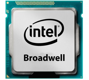
Now, the successor to Haswell is Broadwell. There weren’t a whole lot of changes, but some notable improvements. Not only that, but it’s not meant as a “true” replacement since there would be no low-end or budget CPUs based on the Broadwell architecture.
New features are primarily video-related. With Broadwell, you get Intel Quick Sync Video, which adds VP8 hardware encoding and decoding. There’s support for VP9 and HEVC decoding as well. With the changes being pretty video-related, there’s added support for Direct3D 11.2 and OpenGL 4.4, too. As far as clock speed goes, base mainstream processors start out at 3.1GHz and can be Turbo Boosted to 3.6GHz. Performance variants have a base of 3.3GHz, but can be Turbo Boosted to 3.7GHz.
Skylake, Kaby Lake and Cannonlake
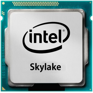
Skylake is the next generation successor to Haswell and Broadwell. It’s one of the most recent variants, having just launched in mid-2015. Now, it is based on the 14nm process, the same process on the Broadwell. But, it does increase CPU and GPU performance across the board while at the same time lowering the power consumption. Skylake was a huge undertaking, but Intel was able to overcome the challenge, bringing us a processor fit for mobile applications all the way up to commercial uses (a TDP of 4.5W to 45W for mobile devices and up to 91W for desktops).
As far as actual features go, you get support for Thunderbolt 3.0, SATA Express and an upgrade to Iris Pro graphics. Skylake actually retires VGA support and adds capabilities for up to 5 displays. Two new instruction sets were also added — Intel MPX, Intel SGX and AVX-512. And on the mobile side of things, Skylake CPUs are actually capable of being overclocked.
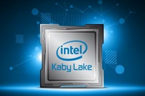
Kaby Lake is the most recent generation of Intel CPUs, having been announced just a few months ago in August 2016. Built on the same 14nm process, Kaby Lake brings much of the trend we’ve already been seeing — better CPU clock speeds and clock speed changes. New graphics architecture was also added to Kaby Lake to improve the performance of 3D graphics and 4K video playback. Beyond that, there weren’t any major changes over Skylake, just a lot of little alterations here and there.
Cannonlake is what will replace the Kaby Lake architecture. We don’t know much about it yet, as it’s been announced, but won’t release until mid-2017. It will be based on the 10nm process, but will be limited in some sense due to the low yields from the 10nm process. That said, Intel plans on releasing Coffee Lake, loosely based on Cannonlake, but with that 14nm process. We don’t know much more beyond that. There are rumors of other replacements coming down the horizon as well — Icelake based on the 10nm process intended to replace Cannonlake in 2018. And finally, Tigerlake based on the 10nm process intended to replace Icelake a year later in 2019.
Click here: Next Page







30 thoughts on “A detailed history of the processor”
In fact, the 8080 external interface was distinctly different from the 8086, in idea, not just width – for example, 8080 pin 21 (DMA acknowledge).
The 8086 was (almost) binary compatible with the 8080 for “regular programs” ie: not ones that twiddled ports nor relied on specific interrupt/trap behaviour.
So where do you draw the line? Where does Bob draw it? WHere does Fiona draw it? All in different places, I suspect.
The author obviously chose to draw their line at the 8086, probably because delving back beyond the original IBM PC machines might not be worthwhile given a presumed intended audience…
“The following chips are considered the dinosaurs of the computer world. PC’s based on these processors are the kind that usually sit around in the garage or warehouse collecting dust. They are not of much use anymore, but us geeks don’t like throwing them out because they still work. You know who you are.”
sounds just like my tech teacher becouse he is always complaining about how things have changed and shows us pictures from back when computers still used tapes and how he used to get paid to change the tapes every two hours for a hospitle